
Get a Quote
Please fill in the form and we will get back to you soon!
We appreciate you contacting iWave.
Our representative will get in touch with you soon!
Get in Touch
We appreciate you contacting iWave.
Our representative will get in touch with you soon!
Xilinx Evaluation Kit
Intel Evaluation Kit
Mircochip Evaluation Kit

Specification
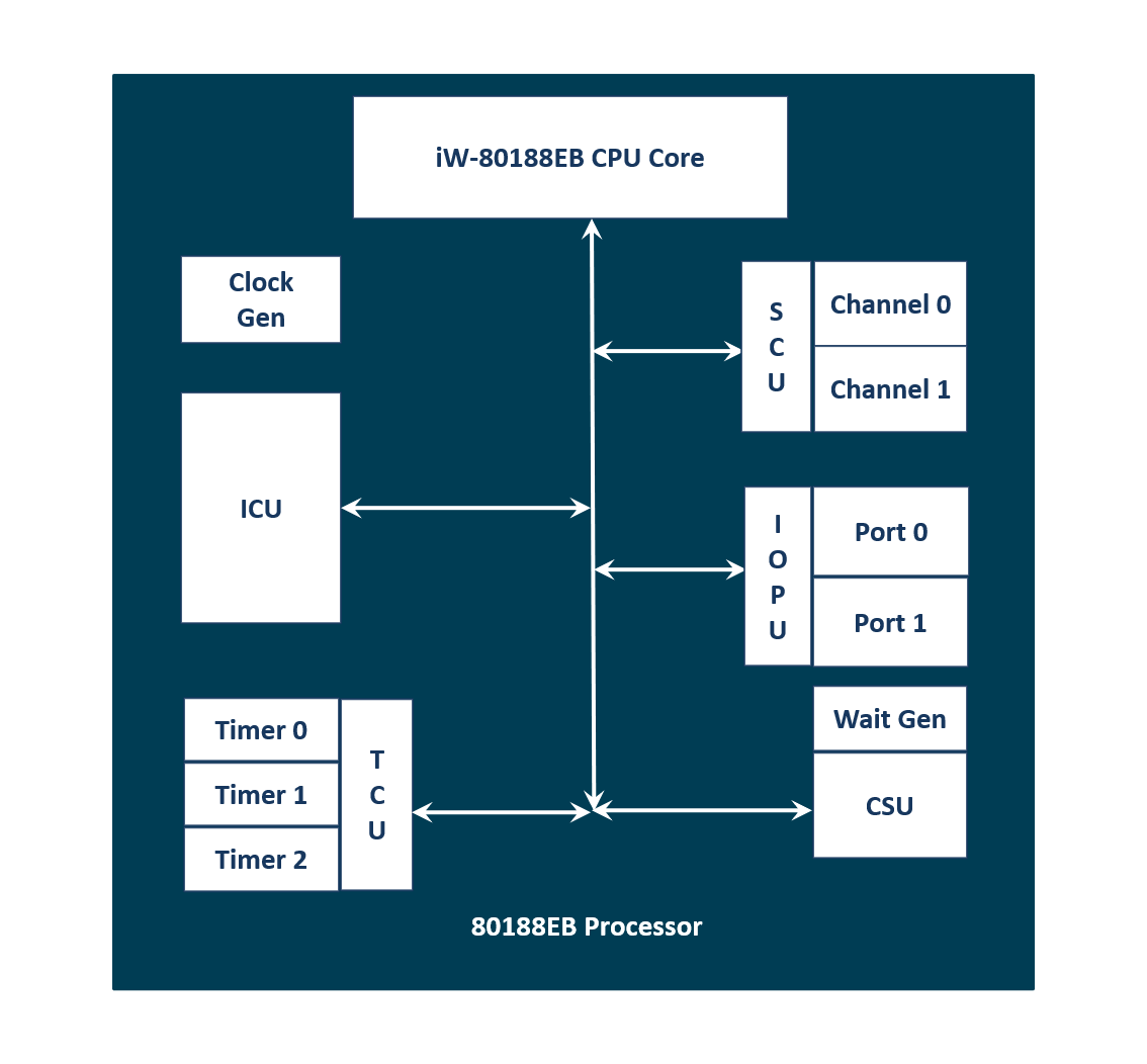
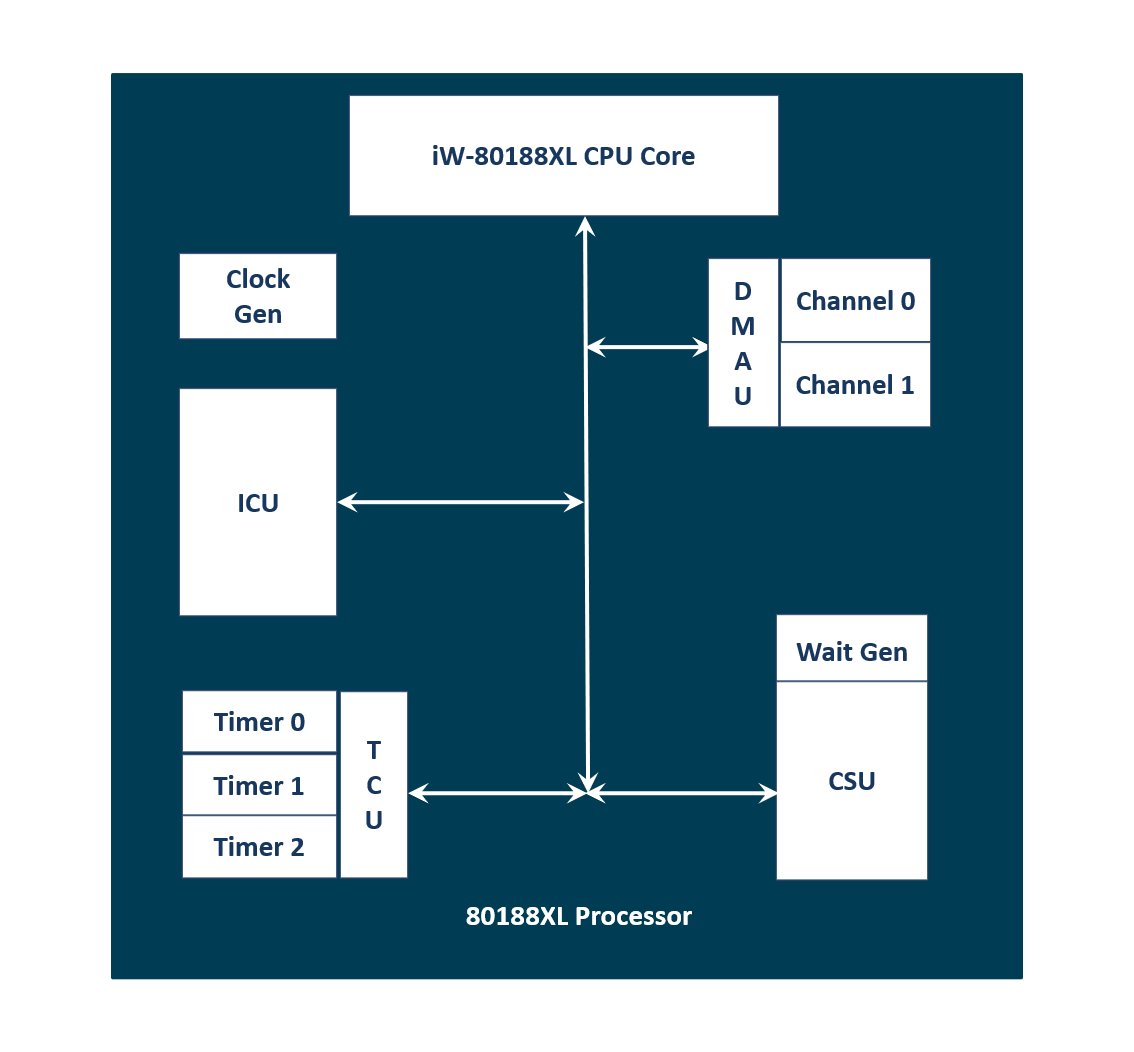
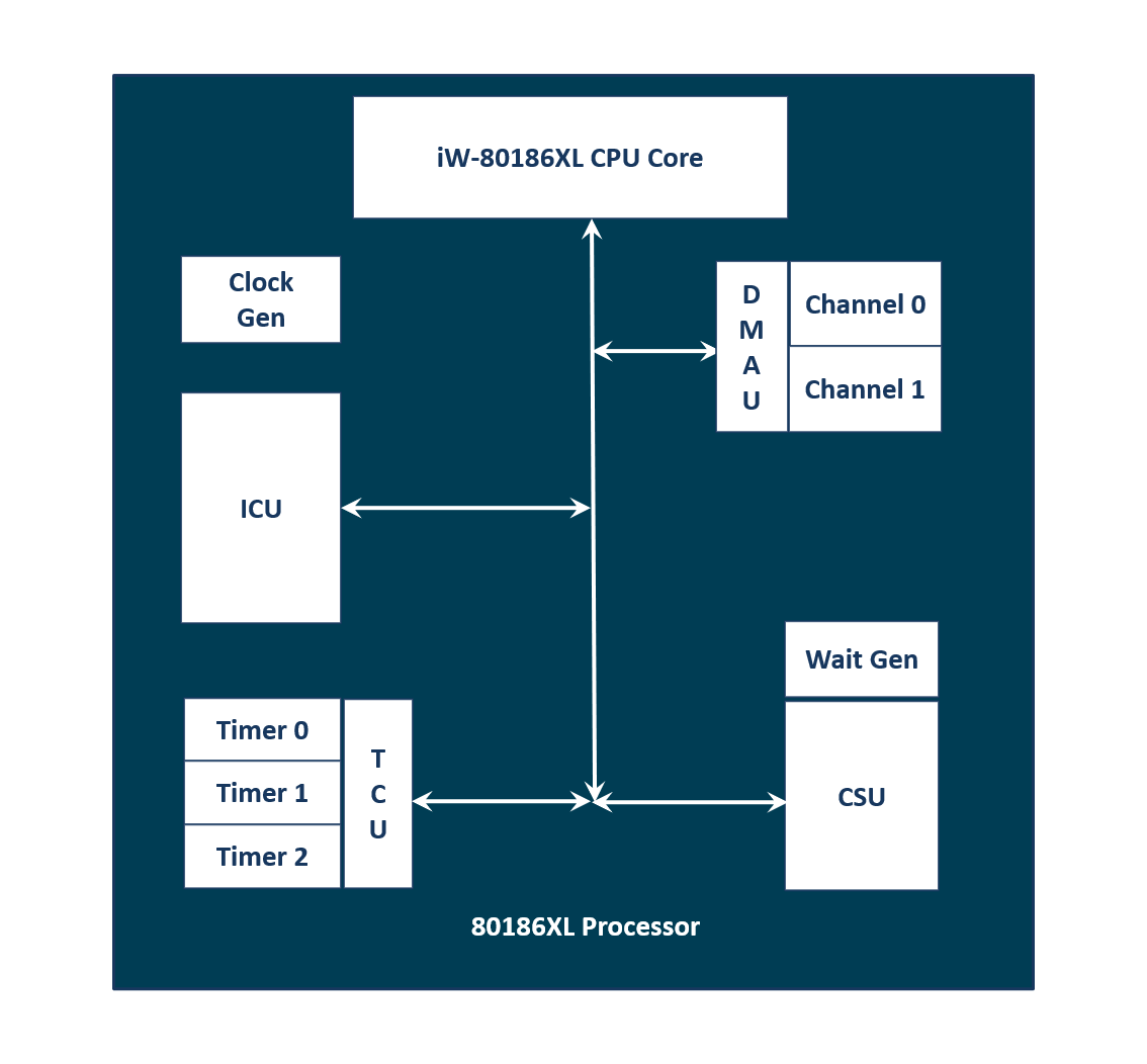
- iW-80186EC CPU Core
- Multiplexed 20-bit address and 16-bit data bus
- 1M-byte memory space divided into 4 segments
- 64K-byte IO space
- Non Maskable Interrupt support
- Arithmetic-Logic Unit
- 8,16,32-bit arithmetic operations
- 8,16-bit logical operations
- Boolean manipulations
- 16 x 16 bit multiplication (signed or unsigned)
- CPU On-Chip Peripherals
- Programmable Timer / Counter Unit
- Three programmable independent 16-bit timers
- TOUT0 to TOUT1 pin outputs
- TIN0 & TIN1 used either as clock or control signals
- Timer-2 can be used to clock other two timers
- Internal / external input clock selectable
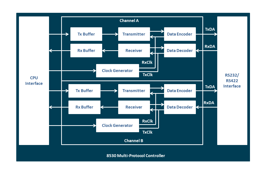
- Serial Communications Unit
- RS-232-C protocol support (on-chip CTS_N, SINT_N pins)
- Only asynchronous mode is supported
- Two independent identical channels
- Full duplex operation in asynchronous mode
- Programmable seven, eight or nine data bits in asynchronous mode
- Independent baud rate generator
- Double-buffered transmit and receive
- Clear-to-Send feature for transmission
- Break character transmission and detection
- Programmable even, odd or no parity
- Detects both framing and overrun errors
- Supports interrupt on transmit and receive
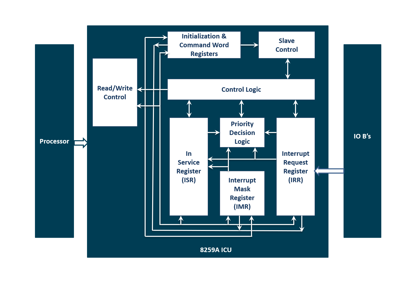
- Interrupt Controller Unit
- Edge trigger / level trigger selectable
- Individually maskable interrupt requests
- Programmable interrupt request priority orders
- Supports Cascading and polling mode
- 8 external interrupt request inputs (INTx ; x=0,1,2,..,7)
- 7 internal interrupt input pins (SCU, TCU, and DMAU)
- Chip Select Unit
- Ten programmable chip-select outputs
- Programmable start and stop addresses
- Memory or I/O bus cycle decoder
- Programmable wait-state generator
- Provision to disable a chip-select
- Provision to override bus ready
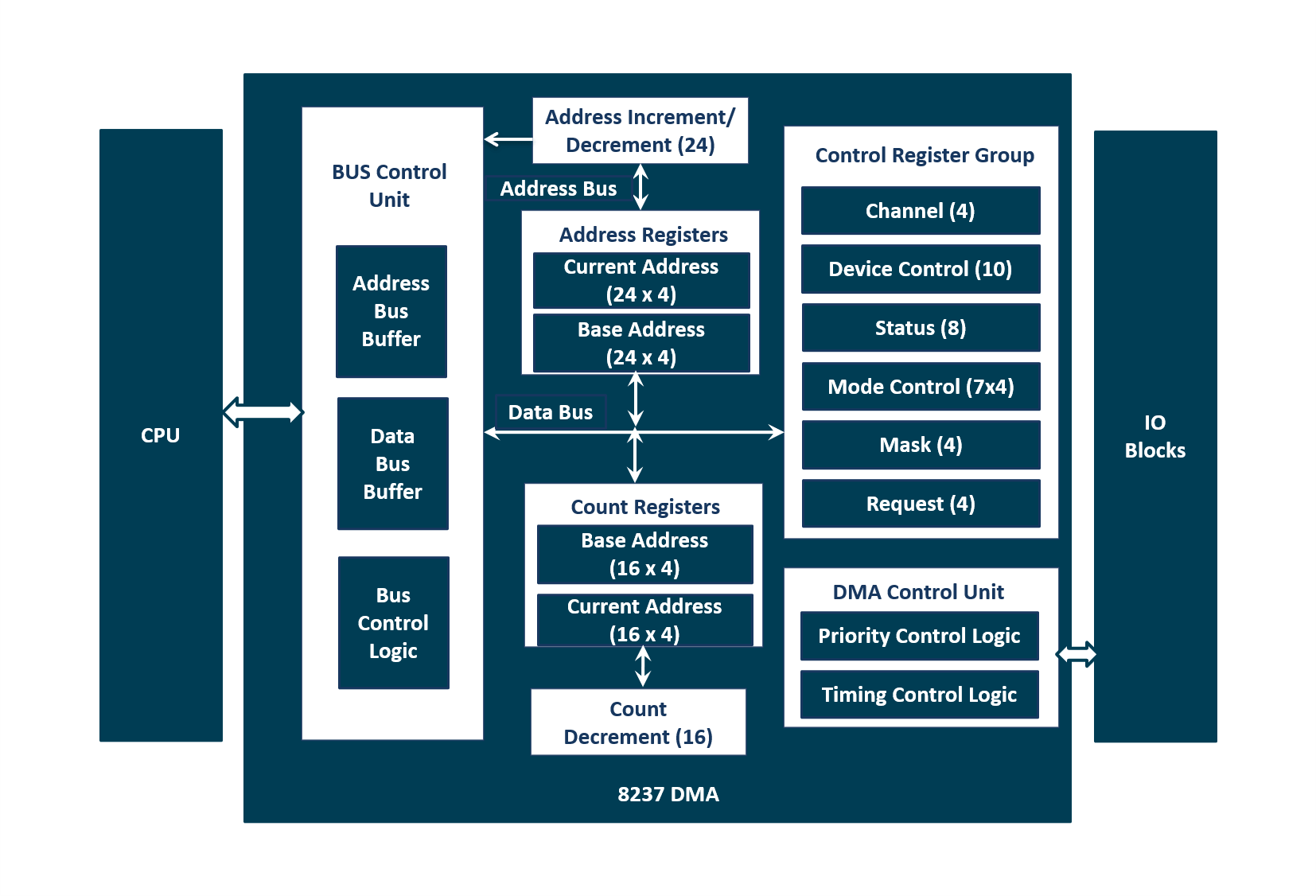
- Direct Memory Access Unit
- Four DMA channels can be accessed independently
- Priority of channels can be modified using priority registers
- DMA requests can be masked by DMA HALT registers
- Four separate External DMA requests pins
- Internal requests either by timer
- programmable software request to start the DMA
- The four channel DMAs are integrated using two channel module
- Watchdog Timer Unit
- 32-bit down counter used,
- Reload and disable option for the watchdog timer
- Asserts a signal to indicate if the program hangs, or some infinite loop occurs
- Multiplexed general purpose Input Output port
- Three ports of total having 22 pins
- A 8 pin inout port multiplexed with the Serial controller unit
- A 8 pin output port multiplexed with Chip Select Unit
- A 6 pin output port multiplexed with DMA and SCU interrupts(4 pins ) and two pins as general purpose inouts
- Clock Generator
- Programmable Timer / Counter Unit
- iW-80186EC CPU Core
Related products

Download
Please fill in the form below to download the document.
Thanks for filling in the download form.
Request Document
Please fill in the form below and we will get back to you soon!
We appreciate you contacting iWave.
Our representative will get in touch with you soon!
iWave is an embedded systems engineering and solutions company, designing solutions for the Industrial, Medical, Automotive and Avionics vertical markets, and building on our core competency of embedded expertise since 1999. Read More…