
Get a Quote
Please fill in the form and we will get back to you soon!
We appreciate you contacting iWave.
Our representative will get in touch with you soon!
Get in Touch
We appreciate you contacting iWave.
Our representative will get in touch with you soon!
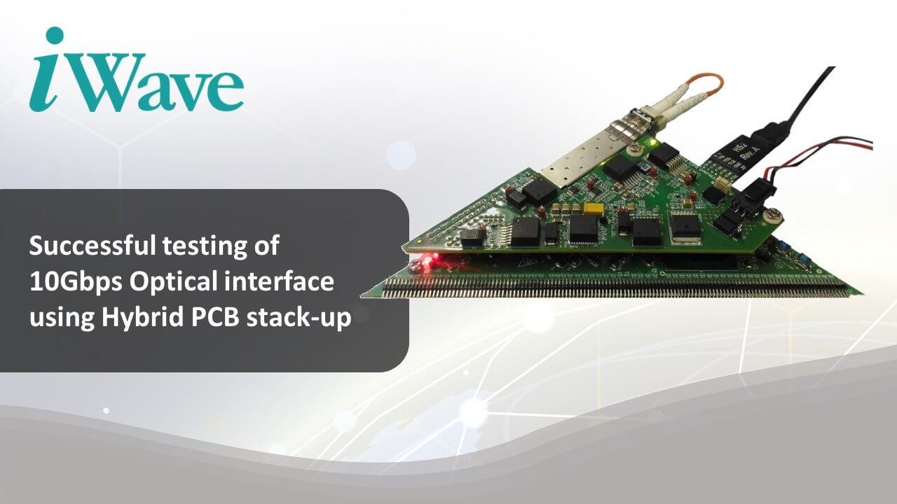
Successful testing of 10Gbps Optical interface using Hybrid PCB stack-up
We have successfully tested a prototype board, capable of establishing communication link 9.95328Gbps upstream and downstream speed, with an optical transceiver module (SFP+ Package) interfaced to GTX transceiver block of the Kintex 7 FPGA.
High-speed FPGA designs at data rates of 10 Gbps and higher require careful attention to material selection and layer stack planning to ensure a robust PCB design. Normally, a low loss PCB stack-up costs more than FR4 stack-up. However, from SI design perspective, not every IO needs low loss. Therefore, if a PCB stack-up is designed with some layers as low loss but other layers in traditional FR4(high loss), then it can meet the same or similar low loss performance requirement for the IOs but at a lower cost that an all low loss board. Such type of stack ups is called hybrid PCB stack-up. Uniqueness of this design lies in the fact that we have used the 12 layer hybrid stack up for cost optimisation, where outer layers are with High speed material Rogers 435O & inner cores are standard FR-4 material.
To verify the Interface, optical loopback test was carried out using Xilinx IBERT IP. The LogiCORE™ IP Integrated Bit Error Ratio Tester (IBERT) core for 7 series FPGA GTX transceivers is designed for evaluating and monitoring the GTX transceivers. This core includes pattern generators and checkers that are implemented in FPGA logic, and access to ports and the dynamic reconfiguration port attributes of the GTX transceivers. Optical loopback cable is used for testing, as shown in Figure below. IBERT IP example design is used to verify the optical interface operating at 9.9533Gbps line rate.
![]()
![]()
Figure 1: Optical transceiver module with loop back cable connected
The purpose of the IBERT IP example design is to:
- Provide a quick demonstration of the customized core instance operating in hardware through the use of a link status indicator based on PRBS generators and checkers which are part of core and generated during IP generation.
- Provide a system which includes reference clock buffers and example system-level constraints.
- Speed up hardware bring-up and debug through the inclusion of a pattern generator and checker.
The example design contains configurable PRBS generator and checker modules per transceiver channel that enable simple data integrity testing and resulting link status reporting. The example design is also synthesizable so it can be used to check for data integrity and hardware links, either through loopback or connection to a suitable link partner. All key status signals, driving basic control signals and hardware I/O interaction can be done using the Serial I/O Analyzer from the Vivado Hardware Manager after downloading the example design generated bit file. Test results captured for optical interface loopback in IBERT can be seen below.
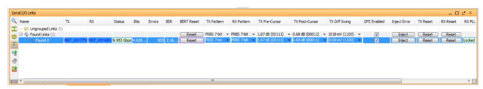
Figure 2: IBERT result when loopback is connected
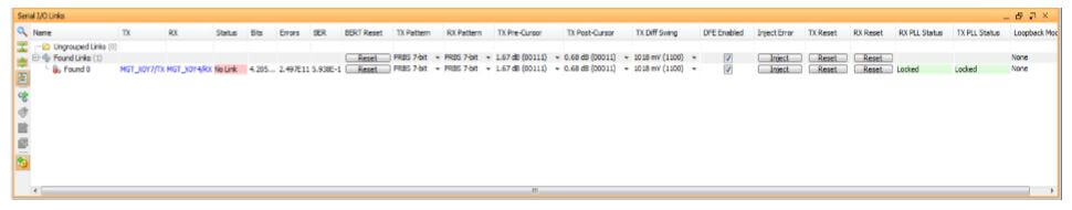
Figure 3: IBERT result when loopback is removed
Therefore Hybrid stack up used here offers two key advantages:
- Better performance compared to all FR4 layer stackup.
- Cost reduction in comparison to stack-ups with low loss PCB material used for all layers.
For further information or enquiries please write to mktg@iwavesystems.com or contact our Regional Partners.
iWave is an embedded systems engineering and solutions company, designing solutions for the Industrial, Medical, Automotive and Avionics vertical markets, and building on our core competency of embedded expertise since 1999. Read More…