Adaptable JESD204B Data Acquisition and Processing Solution from iWave
High-speed real-time data acquisition and processing form the fundamental part of all innovative design developments. Taking this into account, iWave Systems has successfully developed and demonstrated a high-speed analog data acquisition and processing system over the JESD204B serial interface on our Zynq® UltraScale+™MPSoC Development Platform. The JESD204B interface offers seamless connectivity between the AD-FMCDAQ2-EBZ data converters and Zynq Ultrascale+ MPSoC platform, accelerating the development of analog-based designs.
The Zynq Ultrascale+ MPSoC Development Platform :
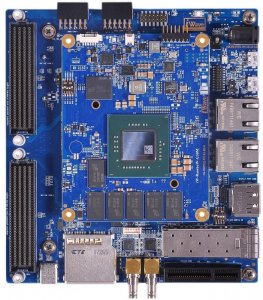
iWave’s Zynq Ultrascale+ SoC Development Kit comprises of Xilinx Zynq Ultrascale+ MPSoC SOM and high-performance carrier card. The SOM is equipped with 64-bit 4GB DDR4 RAM with ECC for PS & 16-bit 1GB for PL. The carrier board supports a rich set of features like FMC (HPC) Connectors, SATA, SFP+, Display Port, USB-Type-C and PCIe x4 connector.
Key Features:
- Zynq Ultrascale+ MPSoC with 504K Logic Cells
- Gigabit Ethernet PHY
- USB2.0 Transceiver
- PS Transceivers x 4 @ 6Gbps
- PL Transceivers x 16 @ 16.3Gbps
- FMC HPC Connector x 2
- Dual 12-Bit PMOD Connectors
- SFP+ Connector
Xilinx Zynq Ultrascale+ SoC suites aptly for the Data Acquisition and Processing Application over JESD204B due to the following key attributes:
- The Xilinx platforms incorporate flexible FPGA transceiver architecture with ready to use JESD204B protocol support that takes care of the required line rate, adaptive gain control (AGC), equalization (EQ) and clock/data recovery (CDR) which are required before converting the data from serial to parallel format.
- For higher data transmission, FPGA transceiver architecture provides pre-emphasis on the Tx to reduce the effects of the inter-symbol interface (ISI) and on the Rx – eye mask specification requirement is achieved with the equalization.
The JES204B interface offers the following key benefits in embedded systems:
- Standardized interface (JEDEC) for data converters
- Simplified interconnect with reduced board space, noise & power.
- An optimized footprint on the PCB allows multiple converters on the same board.
- Up to 12.5 Gbps lane rate
- Uses 8b/10b encoding for SerDes synchronization, clock recovery, and DC balance
- Multi-Lane Synchronization, Multi-Device Synchronization
- Deterministic Latency
- Harmonic Clocking
- Scalable to higher frequencies
- Simplified interface timing
The combination of JESD204B compliant AD-FMCDAQ2-EBZ module and Zynq® UltraScale+™ development board allows quick prototyping and development of FPGA based design solutions that require high-speed data acquisition. Advance use cases include Test and measurement equipment, Radar/Lidar systems, 4G/5G solutions, General-purpose software-defined radios (SDR), Motor control, High-speed data transfer, Ultra-wideband satellite receivers and more.
Demo description:
| FPGA platform | iW-RainboW-G30M ZU7 Zynq UltraScale+ MPSoC |
| Analog input | Sine wave, 25MHz, 1.7Vp-p from signal generator via BNC connector |
| ADC | AD9680, 14-Bit, 1 GSPS, Dual-channel |
| DAC | AD9144, 16-Bit, 2.8 GSPS, Quad-channel |
| FMC Card | Analog Devices – AD-FMCDAQ2-EBZ, HPC-FMC based module with JESD clocking and an SMA connector for analog channels |
| Data Capture | Mixed Domain Oscilloscope with time & frequency domain representation |
| The Demo Consists of Two Data Paths | Demo 1 & Demo 2 |
Demo 1:
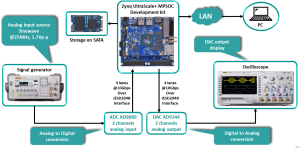
External raw analog data capture from ADC and sent to FPGA-SoC for processing and storing, processed data is sent back to the external world in analog form over DAC.
System Architecture
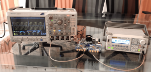
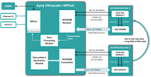
Analog data in the form of a sine wave is provided by the signal generator to the ADC, FPGA captures the digitized data from ADC over JESD204B interface and is sent to SoC for further processing and also optional logging onto on-board mounted M.2 SATA memory as well as a stream over Ethernet interface for further data analysis. On-board 4Gb DDR4 is used for buffering and other data manipulation by the SoC.
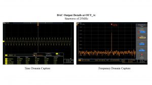
The ADC captured data is sent to DAC via JESD204B interface and analog output is displayed on the Mixed Domain Oscilloscope in frequency & time domain.
Demo 2:
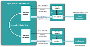
Data generator internal to FPGA-SoC generates the known data pattern, which is sent over DAC to the external world and the analog data is looped back and received into the FPGA-SoC through ADC and post-processing of the captured digitized data and optional storing.
Data Pattern Generator pumps the data stored in the internal RAM to the DAC over the JESD204B interface, AD9144 DAC will do the conversion. The analog output from the DAC is looped back to the ADC using SMA cables. FPGA captures the digitized data from ADC over the JESD204B interface and sent to SoC for further processing. On-board 4Gb DDR4 is used for buffering and processed data will be stored in on-board mounted M.2 SATA memory as well as a stream over Ethernet interface for further data analysis and verification using the GNU plot application at the Host PC.
DAC output Details:
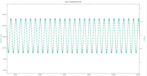
A 25MHz Sine wave digital pattern has been sent to DAC, which will have 40 samples per each crest and trough.ADC captured data plotted on the GNU plot application verifies the number of the samples per each crest and trough and ADC’s input voltage range 1.7Vp-p also can be seen at the GNU plot’s Y2 axis.
ADC captured data on GNU plot
iWave Systems has the stock of various Zynq® UltraScale+™ MPSoC SOM, and we also provide reference binary for the customers who would like to evaluate the AD-FMCDAQ2™ -EBZ Card.
With 20+ years of valuable expertise in the FPGA domain, iWave Systems assures a strong & unparalleled FPGA design-to-deployment competence. As a turnkey product design firm, we offer FPGA designs tailored to meet client’s specifications which includes RTL Design, integration of iWave’s or 3rd Party IP Cores on our FPGA SOMs with carrier card/custom hardware / off-the-shelf evaluation kits to provide end-to-end solutions targeting low-power, high-performance and optimized designs.
More details on iWave’s Zynq MPSoC Module is available here.
For further information or inquiries, please write to mktg@iwavesystems.com or contact our Regional Partners.


