
Get a Quote
Please fill in the form and we will get back to you soon!
We appreciate you contacting iWave.
Our representative will get in touch with you soon!
Get in Touch
We appreciate you contacting iWave.
Our representative will get in touch with you soon!
Documents
Design Support
Application Notes
Software

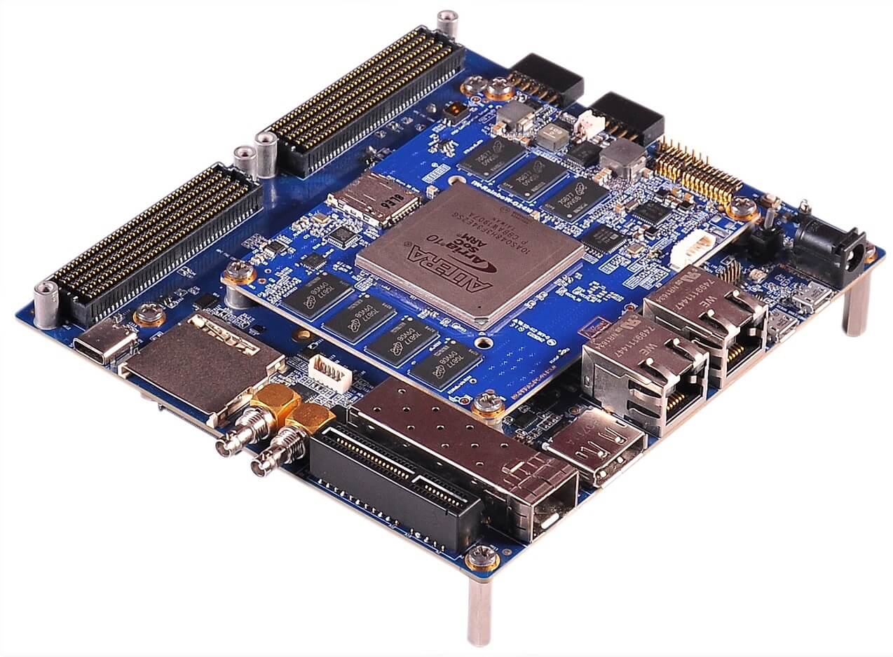
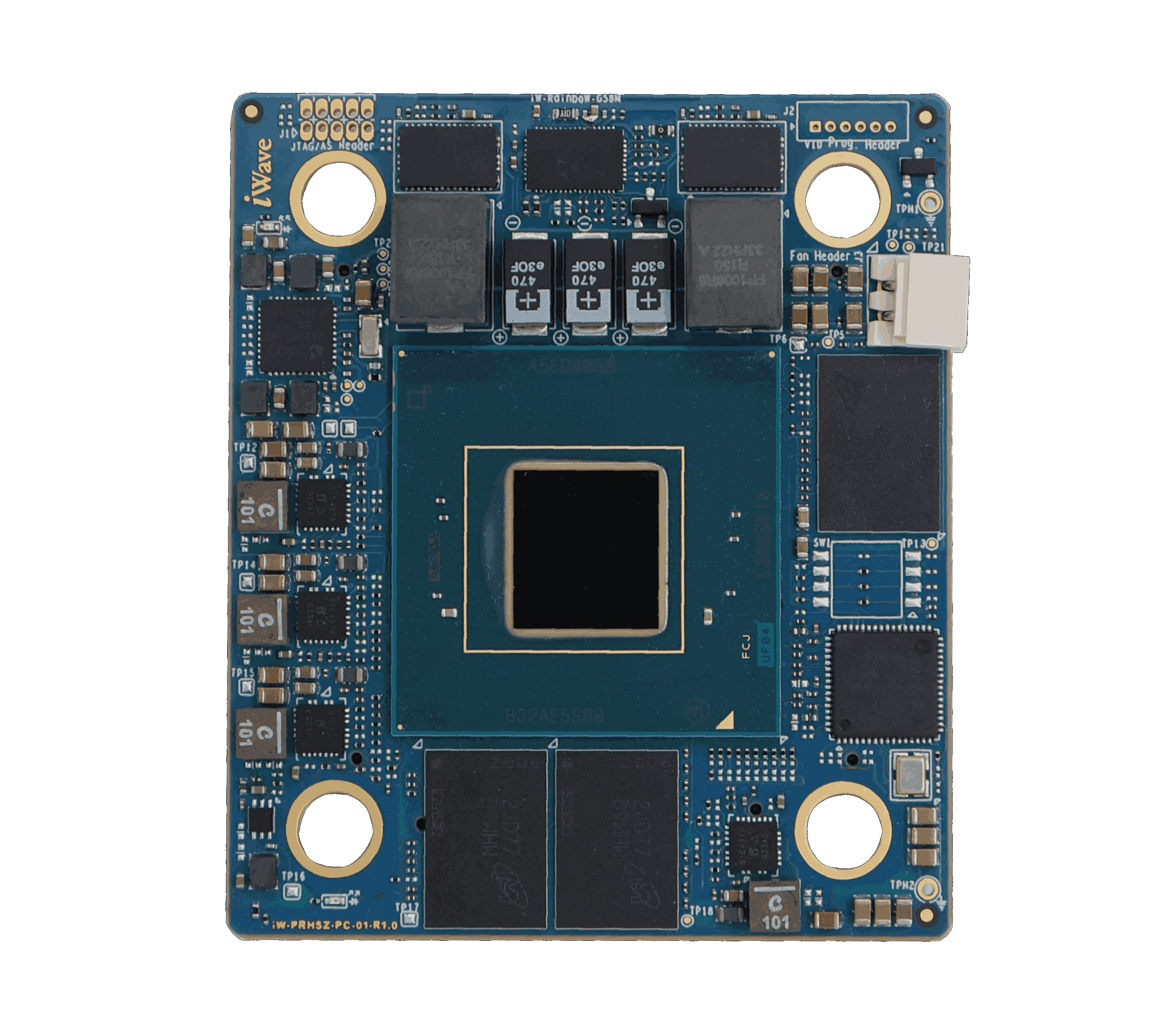
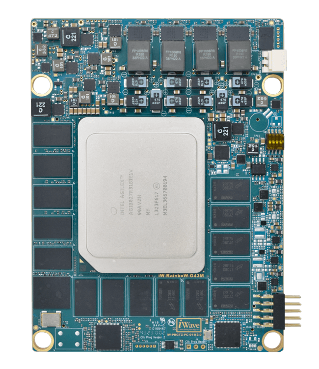
On Module Feature:
|
Two 240pin High Speed Board to Board Connectors Interfaces
| From connector 1 interface |
|
|---|---|
| From connector 2 interface |
|
General Features:
| Power Input | 5V |
|---|---|
| Operating Temperature | -40°C to +85°C |
| Form Factor | 75mm x 95mm |
| BSP Support | Linux BSP:- Linux 5.4/Quartus 21.3 |
| Environment Specification | RoHS &REACH Compliant |
| Compliance | CE* |
Related products
Related products


Download
Please fill in the form below to download the document.
Thanks for filling in the download form.
Request Document
Please fill in the form below and we will get back to you soon!
We appreciate you contacting iWave.
Our representative will get in touch with you soon!
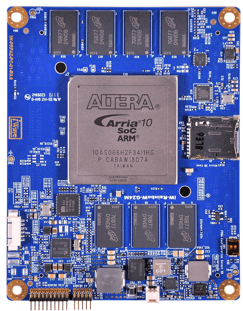
Arria 10 FPGA SOM
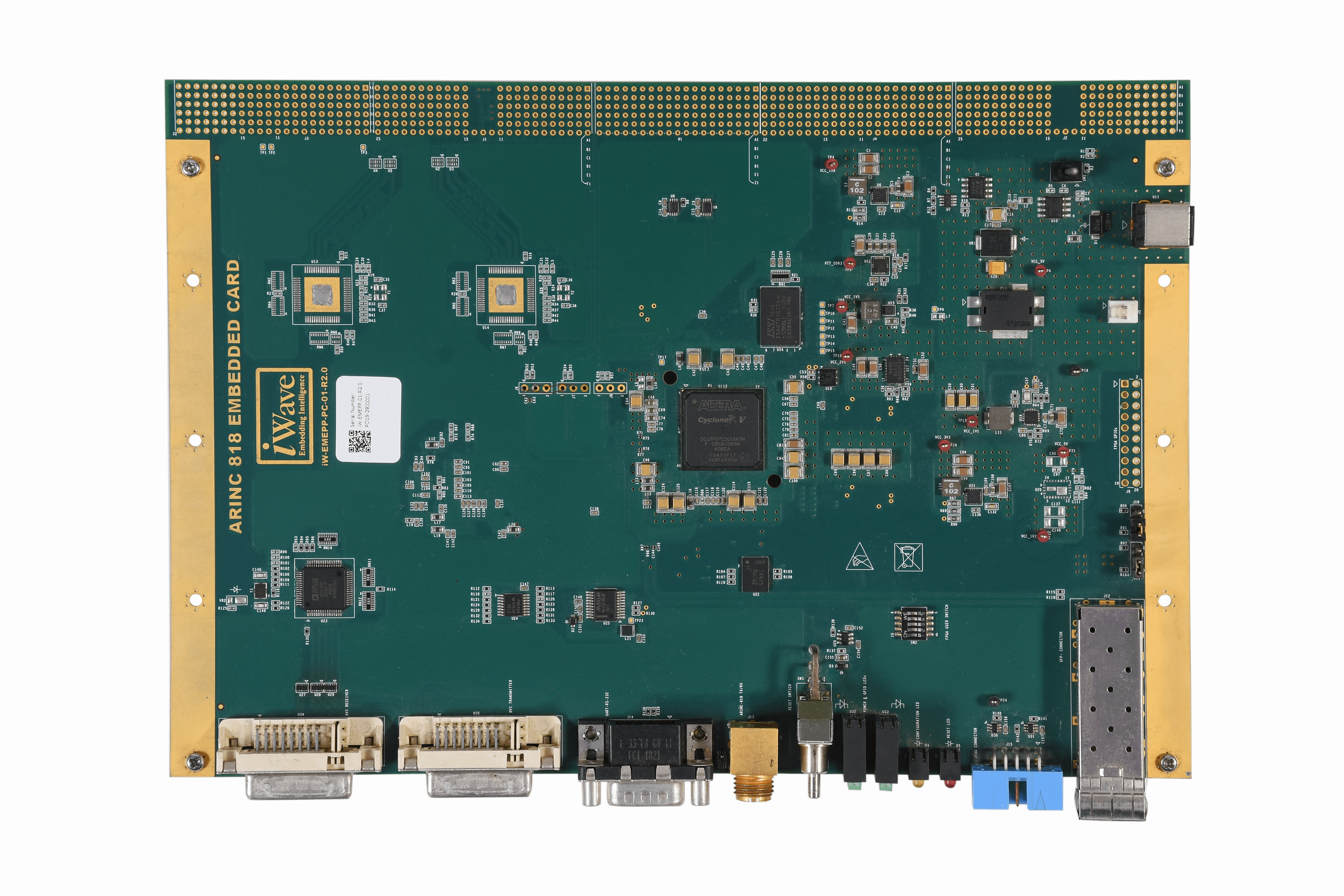
Development Kit
Development Kit
iWave is an embedded systems engineering and solutions company, designing solutions for the Industrial, Medical, Automotive and Avionics vertical markets, and building on our core competency of embedded expertise since 1999. Read More…